User:John R. Brews/Draft: Difference between revisions

From Citizendium
Jump to navigation Jump to search
imported>John R. Brews
No edit summary
Line 1: Line 1:
<br>
<br>
{{Image|Fermi function.PNG|right|300px|Fermi occupancy function ''vs''. energy departure from Fermi level in volts for three temperatures; degeneracy factor ''g''&nbsp;&equiv;&nbsp;1.}}
{{TOC|right}}
{{TOC|right}}
{{Image|MOS Capacitor.PNG|right|250px|Cross section of MOS capacitor showing charge layers}}
==MOS Capacitor==
The '''MOS capacitor''' or '''metal-oxide semiconductor''' capacitor is a two terminal device consisting of three layers: a metal ''gate'' electrode, a separating insulator (often an oxide layer), and a semiconducting layer called the ''body''. The device operates using the [[field effect]], that is, the modulation of the surface conductivity of the semiconductor body by means of an applied voltage between the gate and the body.


==Fermi function==
==Operation==
 
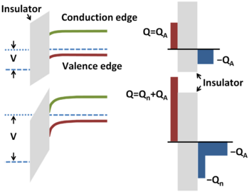
{{Image|Seimiconductor band bending.PNG|right|350px|''Field effect'': Top panels: An applied voltage bends bands, depleting holes from surface (left). The charge inducing the bending is balanced by a layer of negative acceptor-ion charge (right). Bottom panel: A larger applied voltage further depletes holes but conduction band lowers enough in energy to populate an inversion layer.}}
The '''Fermi function''' or, more completely, the '''Fermi-Dirac distribution function''' describes the occupancy of a electronic energy level in a system of electrons at equilibrium. The occupancy ''f(E)'' of an energy level of energy ''E'' at an [[absolute temperature]] ''T'' in [[Kelvin (unit)|kelvin]]s is given by:
 
:<math>
\begin{align}
f(E) &= \frac{1}{1+\exp\left(\frac {E-E_F}{k_B T}\right )} \\
 
&=\frac{1}{1+\exp\left(\frac {(E-E_F)/q}{k_B T/q}\right )}\\
\end{align}
 
</math>
Here ''E<sub>F</sub>'' is called the ''Fermi energy'' and ''k<sub>B</sub>'' is the [[Boltzmann constant]]. This occupancy function is plotted in the figure versus the energy ''E−E<sub>F</sub>'' in eV (electron volts). From the second form of the function above, it can be seen that the "natural" unit of energy is the ''thermal voltage k<sub>B</sub>T/q''; as temperature increases, so does this unit, accounting for the stretching out of the function along the energy axis with increasing temperature.
 
Notice that for an energy level with ''E&nbsp;=&nbsp;E<sub>F</sub>'' and a degeneracy factor ''g''&nbsp;=&nbsp;1, the occupancy is 1/2 regardless of temperature. The Fermi level ''E<sub>F</sub>'' thus can be referred to as the ''half-occupancy'' level.
 
===Dopant levels===
Dopant impurities are used in [[semiconductor]]s to adjust the conductivity of the material. They introduce energy levels for electrons, and if they are ''acceptors'' become negatively charged when occupied. Suppose energies are measured from the valence band edge in a semiconductor, so the impurity energy level becomes ''E<sub>a,d</sub>&nbsp;=&nbsp;E−E<sub>V</sub>'' and ''E<sub>F</sub>'' is replaced by ''E<sub>F</sub>&nbsp;−&nbsp;E<sub>V</sub>''. Then the occupancy of the impurity level is given by:
 
:<math>f(E_{a,d}) = \frac {1}{1+g(E_{a,d})\exp\left(\frac {E_{a,d}-E_F}{k_B T}\right )} \ , </math>
 
where ''g'' is the so-called ''degeneracy factor''. The origin of the degeneracy factor goes back to the underlying derivation of the Fermi function, which is fundamentally a determination of the most probable way ''n''-electrons can be distributed among ''N'' energy levels while constrained by a fixed energy for the ensemble. In this counting of permutations, the contribution of the impurities is included by making some basic assumptions about the impurity behavior that are essentially empirical in nature. For example, one may postulate that the impurity atoms divide into two populations, one with ''n<sub>i</sub>'' electrons and the other with ''n<sub>i</sub>+1'' electrons. Moreover, we suppose that the electrons on any one atom in the first population may fall into any of ''g<sub>0</sub>'' possible equivalent levels, while for those in the second population there are ''g<sub>1</sub>'' possible levels. Then the degeneracy factor in the Fermi occupancy function is found to be ''g<sub>0</sub>/g<sub>1</sub>''.<ref name=degeneracy>
 
Such a derivation can be found in  {{cite book |title=Deep levels, GaAs, alloys, photochemistry; volume 19 of Semiconductors and Semimetals |editor=Robert K. Willardson, Albert C. Beer |author=David C. Look |chapter=Chapter 2: Properties of semi-insulating GaAs: Appendix B  |pages=pp. 149 ''ff'' |url=http://books.google.com/books?id=-aCAjT8J6mYC&pg=PA149 |isbn=0127521194 |year=1983 |publisher=Academic Press}}
 
 
</ref> 
 
Typically an acceptor provides an energy level related to the valence band structure of the host material. A common case is two levels, one from the "heavy" hole valence band and one from the "light" hole valence band. Thus, the number of negatively charge acceptors, compared to the total number of acceptors, is:
 
:<math>\frac {N_a^-}{N_a} = \frac {1}{1+4\exp\left(\frac {E_a-E_F}{k_B T}\right )} \ , </math>
 
where the ''degeneracy factor'' of 4 stems from the possibility of either a spin-up or a spin-down electron occupying the level ''E<sub>a</sub>'', and the existence of ''two'' sources for holes of energy ''E<sub>a</sub>'', one from the "heavy" hole band and one from the "light" hole band.
 
In contrast to acceptors, ''donors'' become positively charged and tend to give up an electron. The number of positive donors compared to the total number of donors is then:
 
:<math>\frac {N_d^+}{N_d} = \frac {1}{1+2\exp\left(\frac {E_d-E_F}{k_B T}\right )} \ , </math>
 
where now the degeneracy factor is 2 (because of the spin-up or spin-down possibilities for occupancy) and there is typically only one energy level ''E<sub>d</sub>'' associated with the conduction band.<ref name=Reisch>
 
{{cite book |title=High-frequency bipolar transistors: physics, modelling, applications |author=Michael Reisch |url=http://books.google.com/books?id=EMZ3EI52pIQC&pg=PA127 |page=p. 127 |chapter=§2.2.2 Ionization |isbn=354067702X |publisher=Springer}}
 
</ref>
 
==Fermi level==
The ''Fermi level'' or ''Fermi energy'', ''E<sub>F</sub>'', in the Fermi function represents for a system of independent electrons a very special case of the more general notion of an [[electrochemical potential]]. The [[chemical potential]] of a chemical species is the work required to add a particle of that species to an ensemble of particles at constant temperature and pressure. The ''electrochemical potential'' is the same quantity, but for a charged particle that has both chemical and electrical interactions.<ref name= Schmickler>See, for example, {{cite book |title=Interfacial electrochemistry |author=Wolfgang Schmickler |chapter=§2.2 The electrochemical potential |pages=pp. 13 ''ff'' |url=http://books.google.com/books?id=c2fYKNzO01QC&pg=PA13 |isbn=0195089324 |publisher=Oxford University Press |year=1996}}
 
</ref>
 
For a system of independent electrons, this energy is the Fermi energy.
 
==Fermi surface==
{{Image|FCC Fermi surface.PNG|right|250px|Fermi surface in '''k'''-space for a nearly filled band in the face-centered cubic lattice}}
At zero temperature, the energy levels up to the Fermi energy are full, and those below are empty. For an assembly of particles occupying these energy levels, the equation ''E&nbsp;=&nbsp;E<sub>F</sub>'' defines a surface in the space of parameters determining the energy, such as the particle momentum. This surface, separating the filled from the empty energy levels, is called the ''Fermi surface''.
 
For example, for an ideal "gas" of independent electrons, the energy of an electron in the gas is given by:
:<math>E = \frac{(\hbar \mathbf{k})^2}{2 m} \ , </math>
where  ''m'' is the electron mass, and the ''wavevector'' '''k''' is related to momentum '''p''' by '''p'''&nbsp;=&nbsp;''ћ'''''k''', where ''ћ'' is [[Planck's constant]] divided by 2π. The wavevector is related to the [[de Boglie wavelength]] of the particle.
 
For this ideal electron gas, the equation ''E&nbsp;=&nbsp;E<sub>F</sub>'' defines a spherical surface in the space of the wavevector. The energy of an electron in a solid is a more complicated function of the ''wavevector'' '''k'''. In a crystal, far from being spherical, the Fermi surface can be complex indeed.
 
==Notes==
==Notes==
<references/>
<references/>

Revision as of 11:05, 19 January 2011


(PD) Image: John R. Brews
Cross section of MOS capacitor showing charge layers

MOS Capacitor

The MOS capacitor or metal-oxide semiconductor capacitor is a two terminal device consisting of three layers: a metal gate electrode, a separating insulator (often an oxide layer), and a semiconducting layer called the body. The device operates using the field effect, that is, the modulation of the surface conductivity of the semiconductor body by means of an applied voltage between the gate and the body.

Operation

(CC) Image: John R. Brews
Field effect: Top panels: An applied voltage bends bands, depleting holes from surface (left). The charge inducing the bending is balanced by a layer of negative acceptor-ion charge (right). Bottom panel: A larger applied voltage further depletes holes but conduction band lowers enough in energy to populate an inversion layer.

Notes