User:John R. Brews/Devices: Difference between revisions

From Citizendium
Jump to navigation Jump to search
imported>John R. Brews
(Created page with "==Devices== {{Gallery-mixed |caption=Devices |width=200 |lines=5 |Two diode structures.PNG|Mesa diode structure (top) and planar diode structure with guard-ring (bottom). |Planar...")
 
imported>John R. Brews
Line 26: Line 26:
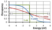
|Fermi function.PNG|Fermi occupancy function ''vs''. energy departure from Fermi level in volts for three temperatures
|Fermi function.PNG|Fermi occupancy function ''vs''. energy departure from Fermi level in volts for three temperatures
|FCC Fermi surface.PNG|Fermi surface in '''k'''-space for a nearly filled band in the face-centered cubic lattice
|FCC Fermi surface.PNG|Fermi surface in '''k'''-space for a nearly filled band in the face-centered cubic lattice
}}
{{Gallery-mixed
|caption=More devices
|width=200
|lines=5
|Silicon conduction band ellipsoids.JPG|A constant energy surface in the silicon conduction band consists of six ellipsoids.
|Planar Schottky diode.PNG|Planar Schottky diode with ''n<sup>+</sup>''-guard rings and tapered oxide.
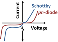
|Schottky & pn diode IV curves.PNG|Comparison of Schottky and ''pn''-diode current voltage curves.
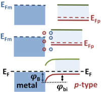
|Schottky barrier height.PNG|Schottky barrier formation on ''p''-type semiconductor. Energies are in eV.
|Schottky barrier (forward bias).PNG|Schottky diode under forward bias ''V<sub>F</sub>''.
|Schottky barrier (reverse bias).PNG|Schottky diode under reverse bias ''V<sub>R</sub>''.
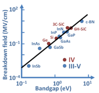
|Breakdown field vs bandgap.PNG|Critical electric field for breakdown ''versus'' bandgap energy in several materials.
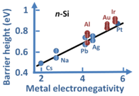
|Schottky barrier vs. electronegativity.PNG|Schottky barrier height ''vs.'' metal electronegativity for some selected metals on ''n''-type silicon.
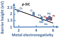
|Schottky barrier on p-SiC.PNG|Theoretical dependence of Schottky barrier heights for diodes using ''p''-SiC ''vs.'' electronegativity of the metal according to Mönch
}}
}}

Revision as of 08:47, 15 July 2011

Devices

Devices
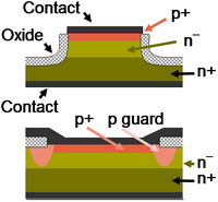
Mesa diode structure (top) and planar diode structure with guard-ring (bottom).
(PD) Image: John R. Brews
Mesa diode structure (top) and planar diode structure with guard-ring (bottom).
A planar bipolar junction transistor as might be constructed in a integrated circuit.
(PD) Image: John R. Brews
A planar bipolar junction transistor as might be constructed in a integrated circuit.
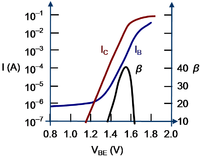
Gummel plot and current gain for a GaAs/AlGaAs heterostructure bipolar transistor.
(PD) Image: John R. Brews
Gummel plot and current gain for a GaAs/AlGaAs heterostructure bipolar transistor.
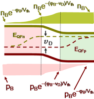
Quasi-Fermi levels and carrier densities in forward biased pn-diode.
(PD) Image: John R. Brews
Quasi-Fermi levels and carrier densities in forward biased pn-diode.
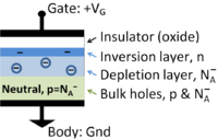
Cross section of MOS capacitor showing charge layers
(PD) Image: John R. Brews
Cross section of MOS capacitor showing charge layers
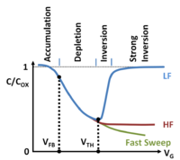
Three types of MOS capacitance vs. voltage curves. VTH = threshold, VFB = flatbands 
(PD) Image: John R. Brews
Three types of MOS capacitance vs. voltage curves. VTH = threshold, VFB = flatbands 
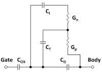
Small-signal equivalent circuit of the MOS capacitor in inversion with a single trap level
(PD) Image: John R. Brews
Small-signal equivalent circuit of the MOS capacitor in inversion with a single trap level
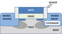
A modern MOSFET
(PD) Image: John R. Brews
A modern MOSFET
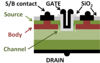
A power MOSFET; source and body share a contact.
(PD) Image: John R. Brews
A power MOSFET; source and body share a contact.
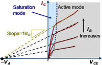
Two bipolar transistor modes, showing extrapolation of asymptotes to the Early voltage.
(PD) Image: John R. Brews
Two bipolar transistor modes, showing extrapolation of asymptotes to the Early voltage.
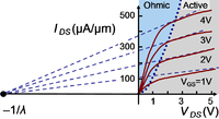
Channel length modulation in 3/4μm technology.
(PD) Image: John R. Brews
Channel length modulation in 3/4μm technology.
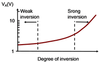
Early voltage for MOSFETs from a 0.18μm process as a function of channel strength.
(PD) Image: John R. Brews
Early voltage for MOSFETs from a 0.18μm process as a function of channel strength.
Calculated density of states for crystalline silicon.
(CC) Image: John R. Brews
Calculated density of states for crystalline silicon.
Field effect: At a gate voltage above threshold a surface inversion layer of electrons forms at a semiconductor surface.
(CC) Image: John R. Brews
Field effect: At a gate voltage above threshold a surface inversion layer of electrons forms at a semiconductor surface.
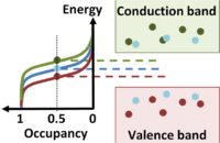
Occupancy comparison between n-type, intrinsic and p-type semiconductors.
(PD) Image: John R. Brews
Occupancy comparison between n-type, intrinsic and p-type semiconductors.
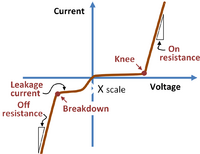
Nonideal pn-diode current-voltage characteristics
(PD) Image: John R. Brews
Nonideal pn-diode current-voltage characteristics
Band-bending diagram for pn-junction diode at zero applied voltage
(PD) Image: John R. Brews
Band-bending diagram for pn-junction diode at zero applied voltage
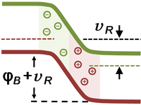
Band-bending for pn-diode in reverse bias
(PD) Image: John R. Brews
Band-bending for pn-diode in reverse bias
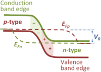
Quasi-Fermi levels in reverse-biased pn-junction diode
(PD) Image: John R. Brews
Quasi-Fermi levels in reverse-biased pn-junction diode
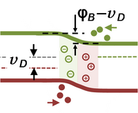
Band-bending diagram for pn-diode in forward bias
(PD) Image: John R. Brews
Band-bending diagram for pn-diode in forward bias
Fermi occupancy function vs. energy departure from Fermi level in volts for three temperatures
(PD) Image: John R. Brews
Fermi occupancy function vs. energy departure from Fermi level in volts for three temperatures
Fermi surface in k-space for a nearly filled band in the face-centered cubic lattice
(PD) Image: John R. Brews
Fermi surface in k-space for a nearly filled band in the face-centered cubic lattice
More devices
A constant energy surface in the silicon conduction band consists of six ellipsoids.
(PD) Image: John R. Brews
A constant energy surface in the silicon conduction band consists of six ellipsoids.
Planar Schottky diode with n+-guard rings and tapered oxide.
(PD) Image: John R. Brews
Planar Schottky diode with n+-guard rings and tapered oxide.
Comparison of Schottky and pn-diode current voltage curves.
(PD) Image: John R. Brews
Comparison of Schottky and pn-diode current voltage curves.
Schottky barrier formation on p-type semiconductor. Energies are in eV.
(PD) Image: John R. Brews
Schottky barrier formation on p-type semiconductor. Energies are in eV.
Schottky diode under forward bias VF.
(PD) Image: John R. Brews
Schottky diode under forward bias VF.
Schottky diode under reverse bias VR.
(PD) Image: John R. Brews
Schottky diode under reverse bias VR.
Critical electric field for breakdown versus bandgap energy in several materials.
(PD) Image: John R. Brews
Critical electric field for breakdown versus bandgap energy in several materials.
Schottky barrier height vs. metal electronegativity for some selected metals on n-type silicon.
(PD) Image: John R. Brews
Schottky barrier height vs. metal electronegativity for some selected metals on n-type silicon.
Theoretical dependence of Schottky barrier heights for diodes using p-SiC vs. electronegativity of the metal according to Mönch
(PD) Image: John R. Brews
Theoretical dependence of Schottky barrier heights for diodes using p-SiC vs. electronegativity of the metal according to Mönch