User:John R. Brews/Draft
Jump to navigation
Jump to search

MOS Capacitor
The MOS capacitor or metal-oxide semiconductor capacitor is a two terminal device consisting of three layers: a metal gate electrode, a separating insulator (often an oxide layer), and a semiconducting layer called the body. The device operates using the field effect, that is, the modulation of the surface conductivity of the semiconductor body by means of an applied voltage between the gate and the body.
Operation

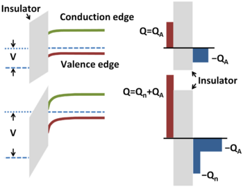
(CC) Image: John R. Brews
Field effect: Top panels: An applied voltage bends bands, depleting holes from surface (left). The charge inducing the bending is balanced by a layer of negative acceptor-ion charge (right). Bottom panel: A larger applied voltage further depletes holes but conduction band lowers enough in energy to populate an inversion layer.
Field effect: Top panels: An applied voltage bends bands, depleting holes from surface (left). The charge inducing the bending is balanced by a layer of negative acceptor-ion charge (right). Bottom panel: A larger applied voltage further depletes holes but conduction band lowers enough in energy to populate an inversion layer.
A device based upon a uniformly doped p-type body is described. The n-type case is similar. The device has four regions of operation depending upon the applied voltage between gate and body:
- Accumulation: For a negative gate bias, holes are drawn to the semiconductor-insulator interface. A conducting surface extends from the bulk all the way to the interface, and the surface conductivity is enhanced by the accumulation of holes at the interface.
- Flat bands: For a specific value of voltage, the bulk hole density is exactly the same from the bulk to the interface. The body is everywhere charge neutral because the hole density exactly balances the acceptor density.
- Depletion: For a positive gate voltage, the holes are pushed away from the positive charge on the gate electrode, and a surface layer depleted of holes is formed extending from the interface to the depth necessary to make the exposed, immobile, negative acceptor ion charge exactly balance the positive charge on the gate. Increase in positive charge on the gate with increasing voltage is balanced by expansion of the depletion layer, increasing the acceptor charge.
- Inversion: For positive gate voltages above a threshold voltage, a surface inversion layer of electrons forms in a narrow layer near the interface. This conducting inversion layer is separated form the p-type neutral bulk by the intervening insulating depletion layer of immobile acceptor charge. Once the gate voltage increases beyond the threshold voltage, additional positive charge on the gate is compensated by increased inversion layer electron charge, and the depletion layer depth no longer expands.